Export controls have forced a radical shift in chip innovation. Huawei is now betting on new design principles to stay competitive. The company's latest approach could redefine how performance is measured in AI hardware.
When access to the world's most advanced chipmaking tools was cut off, Huawei faced a stark choice: fall behind or rethink the fundamentals of semiconductor design. The company’s new approach, unveiled at ISCAS 2026 by semiconductor chief He Tingbo, signals a dramatic pivot in how performance gains are pursued under pressure.
Instead of chasing ever-smaller transistors-a race dominated by TSMC and ASML’s extreme ultraviolet (EUV) lithography-Huawei introduced the Tau (τ) Scaling Law. This framework shifts the focus from geometric scaling to time scaling, prioritizing the reduction of signal delay across chips and systems. In practice, it means reengineering how data moves within and between chips, aiming to cut latency and energy loss by shortening the physical distance signals must travel.
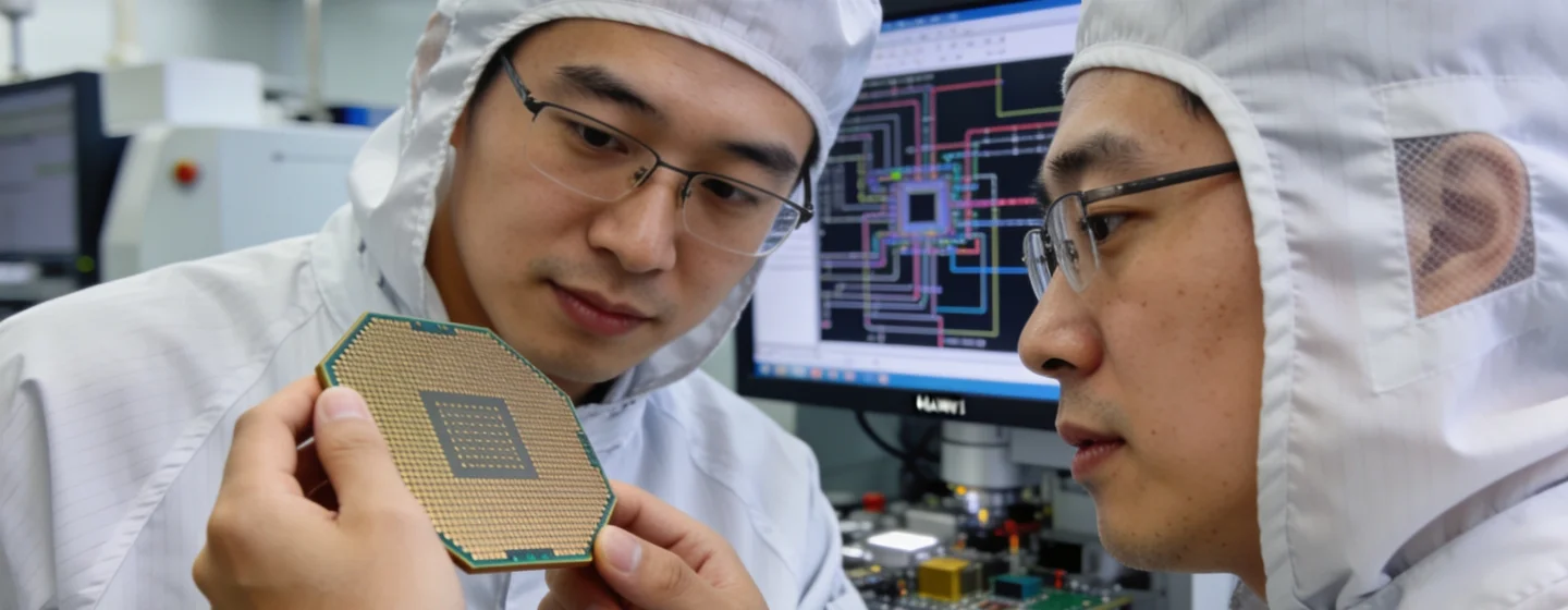
Huawei claims this methodology, refined over six years, has already shaped the design and mass production of 381 chips spanning smartphones, data centers, and automotive applications. The first major test will come with a new Kirin chip, expected in the Mate smartphone line in Fall 2026. If successful, it could demonstrate whether Tau Scaling and the LogicFolding technique-rearranging chip logic to minimize signal paths-can deliver real-world performance at scale. The company has set an ambitious target: by 2031, it aims to reach transistor densities comparable to a 1.4-nanometer process.
He Tingbo likened the strategy to the ancient Dujiangyan irrigation system, which solved a distribution problem by redirecting flow rather than overpowering obstacles. For Huawei, this means redefining what progress looks like when the traditional path-smaller nodes and EUV access-is blocked.
However, the announcement is not evidence that Huawei has matched TSMC’s process technology or Nvidia’s AI accelerator performance. LogicFolding is distinct from standard 3D die stacking; it’s a design-stage method to reduce latency, not just a packaging solution. While advanced packaging and chiplet integration are industry-wide trends, Huawei’s orchestration of these techniques around a single objective-minimizing time and energy costs-sets its approach apart.
Key questions remain: Can Huawei’s designs achieve competitive yields and thermal management? Will independent benchmarks validate the claimed density and performance? And can the company’s ecosystem support the complexity of folded-logic designs at scale? Even the way density is calculated may spark debate, as different formulas can yield different comparisons.
What’s clear is that necessity has forced Huawei to build internal capabilities most firms would outsource. When best-in-class components are unavailable, companies must develop the engineering muscle to align hardware, software, and operations around new technical goals. Constraint alone doesn’t guarantee advantage-it often brings delays and inefficiencies-but with enough resources and market demand, it can drive disciplined innovation.
For Huawei, Tau Scaling also serves as a new coordination tool for suppliers and partners, offering a shared language for progress that isn’t tied solely to EUV access or process nodes. This shift is not about pure self-reliance; post-Moore’s Law scaling will require collaboration across equipment, design, packaging, and software. It also signals a change in Huawei’s external messaging-from proving it can build under pressure to shaping the ecosystem it wants to lead.
Despite these advances, Huawei’s Ascend chips still trail Nvidia’s top products in absolute performance, and production constraints persist. Yet the bigger trend is that Chinese AI developers are increasingly optimizing software and infrastructure for domestic hardware, as access to foreign technology remains uncertain. In this environment, adequacy within a stable ecosystem can outweigh theoretical optimality in one that’s politically off-limits.
This bifurcation is no longer a distant geopolitical issue. Two AI compute ecosystems are now evolving on separate tracks, with different hardware, software, and supply chains. The global frontier remains anchored in ASML, TSMC, and Nvidia, but China’s ecosystem is advancing on its own terms. As seen in recent shifts in AI startup strategies, the ability to adapt to new hardware realities is becoming a core competitive factor.
For companies making AI infrastructure decisions, the choice of ecosystem is now an operational reality, not just a geopolitical abstraction. The question is whether organizations will make that choice deliberately-or simply drift into it as the landscape changes.
Founded in 1987, Huawei Technologies Co., Ltd. has grown into one of the world’s largest technology companies, with over 190,000 employees and operations in more than 170 countries. Despite facing ongoing export restrictions, Huawei reported revenues of 642.3 billion yuan (about $89 billion) in 2025, underscoring its continued influence in global telecommunications and consumer electronics.